circuit diagram of half adder using nand gate
A 16 bit CLA adder can be constructed by cascading four 4 bit adders with two extra gate delays while a 32 bit CLA adder is formed when two 16 bit adders are cascaded to form one system. Ground GND Its the common ground point of the circuit.
Half Adder And Full Adder Circuit With Truth Tables
The equation for SUM requires just an additional input EXORed with the half adder output.
. FA is an easy one-bit adder and if we desire to execute the addition of n-bit then n no. This pin is either grounded or connected to the negative rail. Fig 2 555 Timer IC Pin Diagram.
So we add the Y input and the output of the half adder to an EXOR gate. 4008 4-bit full adder pinout. As their name implies a Binary Subtractor is a decision making circuit that subtracts two binary numbers from each other for example X Y to find the resulting difference between the two numbers.
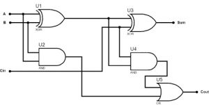
Other examples of combinational switching circuits are half adder and full adder encoder decoder multiplexer de-multiplexer code converter etc. The two gates of XOR and AND followed by one OR gate can be utilized to construct the circuit of a full adder. As with an adder in the general case of calculations on multi-bit numbers three bits are involved in performing the subtraction for each bit of the difference.
Half-subtractor using NAND gate Half-subtractor using NOR gate If we examine the Boolean expressions of the half subtractor with a half adder Then we can figure out that the two expressions for the Sum regarding adder and Difference regarding subtractor are exactly the same and this is because of the Exclusive-OR gate function. 37 Truth Table. The circuit of this can be built with logic gates such as OR Ex-OR NAND gate.
Binary Subtraction The Theory. Unlike the Binary Adder which produces a SUM and a CARRY bit when two binary numbers are added together the binary subtractor produces a DIFFERENCE D by using a. Combinational Circuit- 24 Decoder.
The half adder can add only two input bits A and B and has nothing to do with the carry if there is any in the input. A CLA is termed as the successor of a ripple carry adder. When C 1 both MOSFETs are ON and the signal pass through the gate ie.
So if the input to a half adder. The sum bit and carry bit can be written in terms of NOR operations performed by the logic gates. The Article Gives a BrIef about Carry Look-ahead Adder Truth Table Circuit Diagram Logic Diagram of 4-bit Adder along with Applications Advantages.
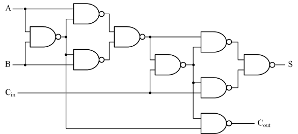
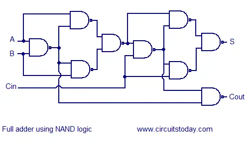
The FA circuit with the NAND gates diagram is shown below. Unfortunately for the 4-bit ALU it would be impractical to use discrete chips to create a 4-bit adder. The half adder adds two single binary digits A and BIt has two outputs sum S and carry CThe carry signal represents an overflow into the next digit of a multi-digit addition.
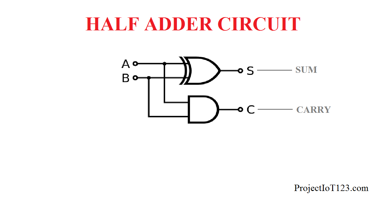
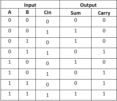
Half Adder and Half Subtractor using NAND NOR gates. 36 Venn Diagram. This table is known as Half adder table as it gives the simple.
Encoders and Decoders in Digital Logic. A carry lookahead adder definition is it is the faster circuit in performing binary addition by using the concepts of Carry Generate and Carry Propagate. Alternative approach - Truth table of a D Flip-Flop- By looking at the circuit diagram it is clear that the boolean expressions of P Q and R are- Here the subscript t refers to the.
Adapted from this image. A0 B0 constitute the binary digit inputs. Large numbers of tiny MOSFETs metaloxidesemiconductor field-effect transistors integrate into a small chipThis results in circuits that are orders of.
Half adder is the simplest of all adder circuit but it has a major disadvantage. In this section CMOS logic circuits that are based on transmission gate are. Likewise the full-subtractor uses binary digits like 01 for the subtraction.
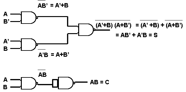
To produce OR gate using NAND gate the inputs A and B of the two NOT gates obtained from the NAND gates are joined together. 38 Canonical Forms for Boolean Function. Digital Logic.
By combining two cells we can perform more complex operations such as the addition of two numbers using a half-adder shown in Fig. Full Adder Design with using NAND Gates. Half Adder using basic gates.
The ground terminal of external circuit as well as power supply V CC ground terminal is connected to the GND terminal of 555 timer. A NAND gate is one kind of universal gate used to execute any kind of logic design. 7101 TTL NAND Gate with Totem-pole Output.
So we will cheat and use a 4008 4-bit adder IC. 4b see Supplementary Tables 4 5 for a breakdown of available. Even the combination of half adders can also lead to the formation of this adder.
OR gate using NAND gate. The circuit for the above equations can be constructed as shown below. Two whole half adder circuits in addition to an OR gate gives rise to a full adder circuit.
A decoder converts the binary coded data at its present input into a number of different output lines. The transmission gate is mainly a bi-directional switch enabled by the gate signal C. Of one-bit FAs must be employed in the cascade.
Similarly for the carry output of the half adder we need to add YAB in an OR configuration. An integrated circuit or monolithic integrated circuit also referred to as an IC a chip or a microchip is a set of electronic circuits on one small flat piece or chip of semiconductor material usually silicon. Encoders and Decoders in Digital Logic.
Full adders are constructed using the basic logic gates. In order to perform these repeated functions adder circuits are required and those are half adder full adder carry lookahead adder. The inputs A and B will get inverted.
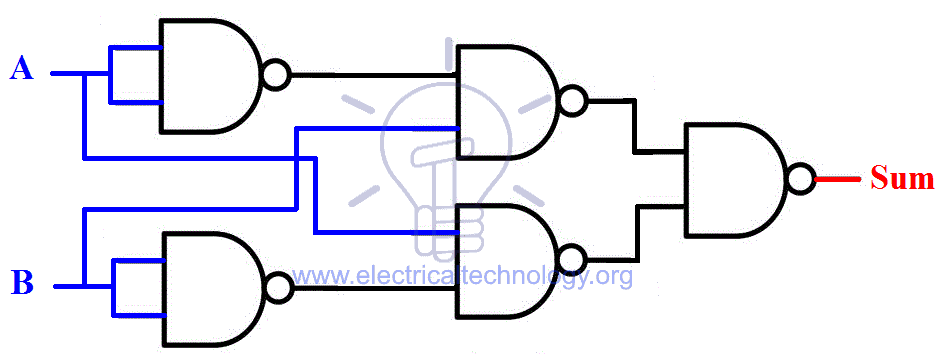
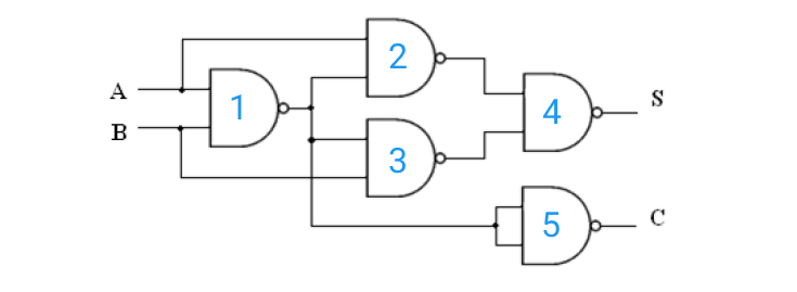
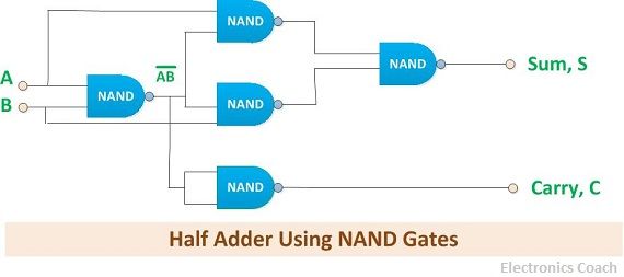
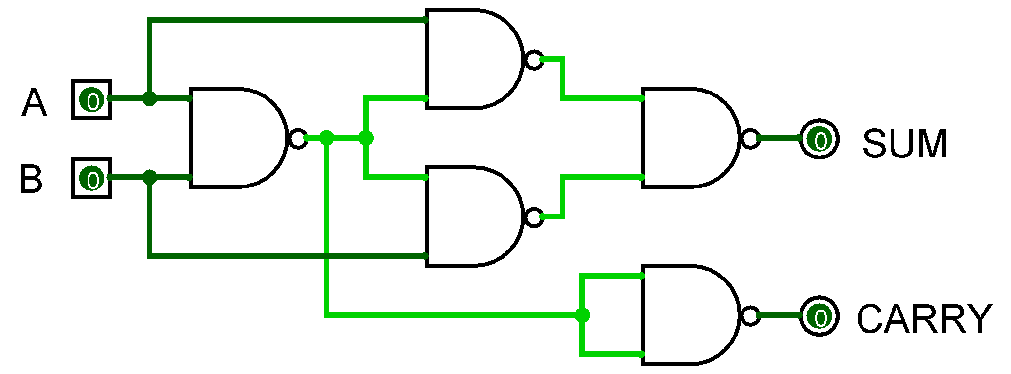
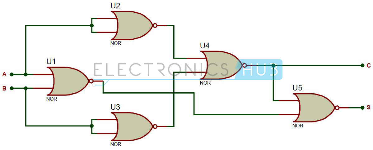
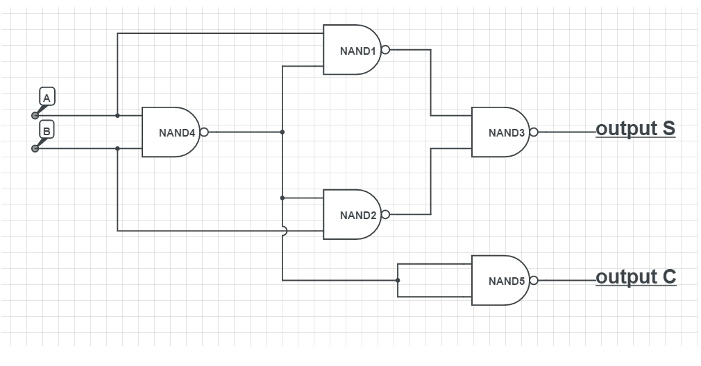
Encoders and Decoders are examples of combinational circuit. This circuit employs seven NAND gates to create a half adder circuit. The key point which is to be kept in mind while designing the circuit using universal gate is that the architecture in which it is to be connected so that it performs the desired operation.
Connection using a resistor is not recommended to avoid heating up of the IC. A full adder made by using two half adders and an OR gate. Different types of Digital systems are constructed from very few types of basic network configurations such as AND gate NAND gate Or gate etcThese elementary circuits are used over.
The Half adder can also be constructed using basic gates such as NOT gate AND gate and OR gate. The total of 5 NAND gate are used for designing of Subtractor circuit. Logic Gates using NAND and NOR universal gates.
Half Adder and Half Subtractor using NAND NOR gates. In PLA all the minterms are not realized but only required. Full Adder Circuit Using Basic Gates.
FA using NAND Gates. The circuits comprise two half adder circuits. A B if C 1.
You can pick these up for a few dollars on eBay. In the following diagram A1 and B1 are the binary digits C0 is the carry from the previous stage S1 becomes the sum C1 is. The operation of the above circuit diagram can be understood more clearly with the help of equation.
In electronics a subtractor a digital circuit that performs subtraction of numbers can be designed using the same approach as that of an adderThe binary subtraction process is summarized below. For the realization of the above function following circuit diagram will be used. In the earlier article already we have given the basic theory of half adder a full adder which uses the binary digits for the computation.
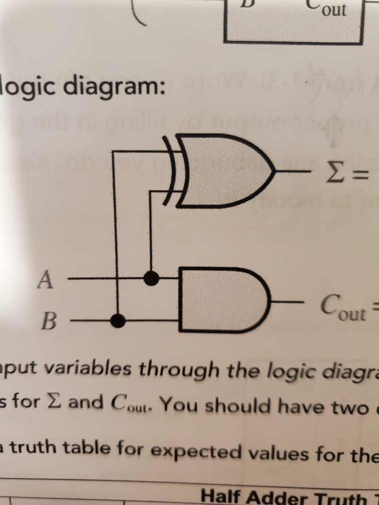
Full Adder using Half Adder. Whereas C 0 makes the MOSFETs cut off creating an open circuit between nodes A and B. The value of the sum is 2C SThe simplest half-adder design pictured on the right incorporates an XOR gate for S and an AND gate for CThe Boolean logic for the sum in this case S will be AB AB.
Similarly NAND gate can also be used to design half subtractor. These outputs are then fed as inputs to the NAND gate as shown in fig. From this it is clear that a half adder circuit can be easily constructed using one X-OR gate and one AND gate.
Compare the equations for half adder and full adder. PLA is used for the implementation of various combinational circuits using a buffer AND gate and OR gate.
Binary Adder Subtractor Construction Types Applications
Deldsim Half Adder Using Nand Gates
Digital Electronics Laboratory
What Is Half Adder Half Adder Using Nand Gates Nor Gates Truth Table Electronics Coach
Half Full Adder Half Full Subtractor Ahirlabs

Implimentation Of Full Adder Using Nand Gate ह न द Youtube
Ripple Carry Adder 4 Bit Ripple Carry Adder Circuit Propagation Delay
Half Adder Circuit And Full Adder Circuit Using Nand Gates

Full Adder In Digital Logic Geeksforgeeks

Instrumentation In A Nutshell Implementation Of Half Adder With Nand Gates
Virtual Labs
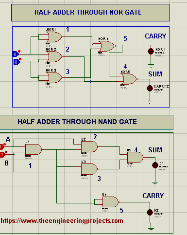
Proteus Simulation Of Half Adder Using Logic Gate The Engineering Projects

Realizing Half Adder Using Nand Gates Only Youtube
Solved Design A Half Adder Circuit Using One Xor Gate And Chegg Com

Logic Gates Go For A
File Half Adder Using Nand Gates Only Jpg Wikimedia Commons
Virtual Labs